鈻?/div>
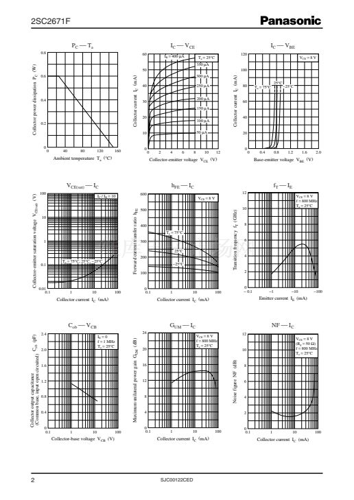
Electrical Characteristics
T
a
=
25擄C
鹵
3擄C
Parameter
Collector-base cutoff current (Emitter open)
Emitter-base cutoff current (Collector open)
Forward current transfer ratio
Transition frequency
Collector output capacitance
(Common base, input open circuited)
Foward transfer gain
Maximum unilateral power gain
Noise figure
Second inter modulation distortion
*
Third inter modulation distortion
*
Symbol
I
CBO
I
EBO
h
FE
f
T
C
ob
錚
21e
錚?/div>
2
G
UM
NF
IM
2
IM
3
Conditions
V
CB
=
10 V, I
E
=
0
V
EB
=
1 V, I
C
=
0
V
CE
=
8 V, I
C
=
40 mA
V
CE
=
8 V, I
C
=
40 mA, f
=
0.8 GHz
V
CB
=
10 V, I
E
=
0, f
=
1 MHz
V
CE
=
8 V, I
C
=
40 mA, f
=
0.8 GHz
V
CE
=
8 V, I
C
=
40 mA, f
=
0.8 GHz
V
CE
=
8 V, I
C
=
40 mA, f
=
0.8 GHz
V
CE
=
8 V, I
C
=
40 mA, f
1
=
200 MHz
f
2
=
500 MHz, V
O
=
100 dB碌/75
鈩?/div>
V
CE
=
8 V, I
C
=
40 mA, f
1
=
600 MHz
f
2
=
500 MHz, V
O
=
100 dB碌/75
鈩?/div>
50
75
9
10
50
3.5
150
5.5
0.8
12
13
2.0
60
86
15
3.2
1.5
Min
Typ
Max
1
1
300
Unit
碌A(chǔ)
碌A(chǔ)
錚?/div>
GHz
pF
dB
dB
dB
dB
Note) 1. Measuring methods are based on JAPANESE INDUSTRIAL STANDARD JIS C 7030 measuring methods for transistors.
2. *: See measurement circuit
f1
Signal generator
Converter (75
鈩?
(50
鈩?
Mixer
(75
鈩?
f2
Signal generator
Converter (75
鈩?
(50
鈩?
DC power
supply
Under
test part
Converter (75
鈩?
(50
鈩?
Spectrum
analyzer
2.3
鹵0.2
Publication date: March 2003
SJC00122CED
1


 1
1
 2
2
 3
3
